- Shop
- GPU cards & Edge AI
- NVIDIA H100 (customized)
-
Overview
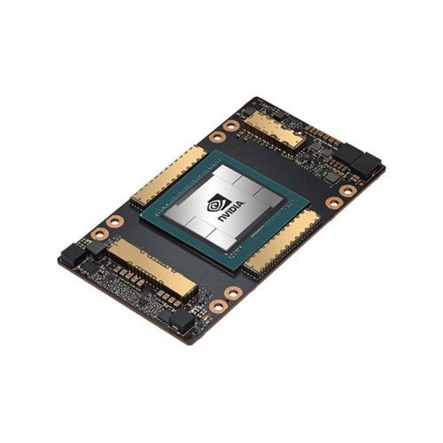
The NVIDIA H100 is a high-end data-centre GPU accelerator designed to meet the demands of large-scale artificial intelligence (AI), high performance computing (HPC), and inference workloads. Built on NVIDIA’s Hopper™ architecture, it delivers exceptional performance, scalability and security for modern data-centre applications.
The H100 is engineered to accelerate everything from training large language models to running high-throughput inference workloads and complex scientific simulations.
It supports both the SXM (high-density server) and PCIe (traditional server slot) form-factors, making it flexible for various deployment scenarios.Features
- Fourth-generation Tensor Cores and dedicated Transformer Engine to dramatically accelerate AI model training and inference.
- Massive memory bandwidth (up to multiple terabytes per second) and large on-board memory (e.g., 80 GB in many configurations) to support large models and datasets.
- Multi-instance GPU (MIG) capability: the GPU can be partitioned into smaller independent instances to handle multiple workloads efficiently.
- High-performance interconnect (e.g., NVLink) enabling multi-GPU scaling and very low latency communication between accelerators.
- Security features such as Confidential Computing capabilities built in, enabling trustworthy execution of sensitive workloads in a shared infrastructure.
- Flexibility of deployment: the H100 is suitable for training, inference, data-centre consolidation, HPC and generative AI workflows.
Specifications
Here are some of the key technical specifications for the NVIDIA H100 (values vary depending on variant: SXM vs PCIe):
Parameter
Value (approximate)
On-board GPU memory
80 GB (common)
Memory bandwidth
Up to ~3.35 TB/s (SXM variant) ~2 TB/s (PCIe variant)
FP64 peak performance
~26 TFLOPS (PCIe)
FP64 Tensor Core performance
~51 TFLOPS (PCIe)
INT8 / FP8 (inference)
Up to ~3 000 TOPS (on PCIe with sparsity)
Maximum thermal design power (TDP)
Up to ~700 W (SXM variant) ~300-350 W (PCIe variant)
Form factor / Interconnect
Variants include SXM and PCIe; NVLink bandwidth up to ~900 GB/s in top configurations.
Multi-GPU scaling
Supports GPU-to-GPU interconnect enabling large clusters (e.g., up to 256 GPUs with NVLink switch system) for exascale workloads.


